ファイル:Wafer flats convention v2.svg

この SVG ファイルのこの PNG プレビューのサイズ: 150 × 150 ピクセル. その他の解像度: 240 × 240 ピクセル | 480 × 480 ピクセル | 768 × 768 ピクセル | 1,024 × 1,024 ピクセル | 2,048 × 2,048 ピクセル。
元のファイル (SVG ファイル、150 × 150 ピクセル、ファイルサイズ: 13キロバイト)
ウィキメディア・コモンズのファイルページにある説明を、以下に表示します。
|
概要
| 解説 |
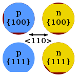
Wafer flats convention, based on Image:Wafer flats convention.PNG Conventional meaning of flats in semiconductor wafers. Red denotes material that has been removed. Wafer orientation is the orientation of the crystallographic plane in which the crystal grew. Wafer type indicated the type of doping.
|
| 日付 | |
| 原典 |
self-made, |
| 作者 | Twisp |
| その他のバージョン | Wafer flats convention.PNG |
ライセンス
| この著作物の著作権者である私は、この著作物における権利を放棄しパブリックドメインとします。これは全世界で適用されます。 一部の国では、これが法的に可能ではない場合があります。その場合は、次のように宣言します。 私は、あらゆる人に対して、法により必要とされている条件を除き、如何なる条件も課すことなく、あらゆる目的のためにこの著作物を使用する権利を与えます。 |
ファイルの履歴
過去の版のファイルを表示するには、その版の日時をクリックしてください。
| 日付と時刻 | サムネイル | 寸法 | 利用者 | コメント | |
|---|---|---|---|---|---|
| 現在の版 | 2013年9月24日 (火) 21:40 | | 150 × 150 (13キロバイト) | Cepheiden | fixed position of secondary flat Silicon processing for the VLSI era - Vol. 1 - Process technology; S Wolf; RN Tauber - Lattice Press; 1986; ISBN 096167237; p. 23 |
| 2008年12月23日 (火) 00:37 |  | 150 × 150 (13キロバイト) | Inductiveload | Added arrow indication <110> direction and enlarged flats so they can be easily seen | |
| 2008年2月29日 (金) 21:17 |  | 150 × 150 (9キロバイト) | Twisp | ||
| 2008年2月29日 (金) 21:13 |  | 150 × 150 (9キロバイト) | Twisp | ||
| 2008年2月29日 (金) 21:06 |  | 150 × 150 (8キロバイト) | Twisp | ||
| 2008年2月29日 (金) 20:59 |  | 150 × 150 (8キロバイト) | Twisp | ||
| 2008年2月29日 (金) 18:09 |  | 150 × 150 (9キロバイト) | Twisp | {{Information |Description= Wafer flats convention, based on Image:Wafer flats convention.PNG Conventional meaning of ''flats'' in semiconductor wafers. Black denotes material that has been removed. Wafer orientation is |
ファイルの使用状況
以下のページがこのファイルを使用しています:
グローバルなファイル使用状況
以下に挙げる他のウィキがこの画像を使っています:
- ca.wikipedia.org での使用状況
- cs.wikipedia.org での使用状況
- de.wikipedia.org での使用状況
- en.wikipedia.org での使用状況
- es.wikipedia.org での使用状況
- et.wikipedia.org での使用状況
- eu.wikipedia.org での使用状況
- fi.wikipedia.org での使用状況
- it.wikipedia.org での使用状況
- it.wikibooks.org での使用状況
- ko.wikipedia.org での使用状況
- nl.wikipedia.org での使用状況
- pl.wikipedia.org での使用状況
- ro.wikipedia.org での使用状況
- sk.wikipedia.org での使用状況
- uk.wikipedia.org での使用状況
- www.wikidata.org での使用状況