ファイル:PCB design and realisation smt and through hole.png
このプレビューのサイズ: 800 × 427 ピクセル。 その他の解像度: 320 × 171 ピクセル | 640 × 341 ピクセル | 1,024 × 546 ピクセル | 1,280 × 683 ピクセル | 3,000 × 1,600 ピクセル。
元のファイル (3,000 × 1,600 ピクセル、ファイルサイズ: 2.74メガバイト、MIME タイプ: image/png)
ウィキメディア・コモンズのファイルページにある説明を、以下に表示します。
|
| 解説 |
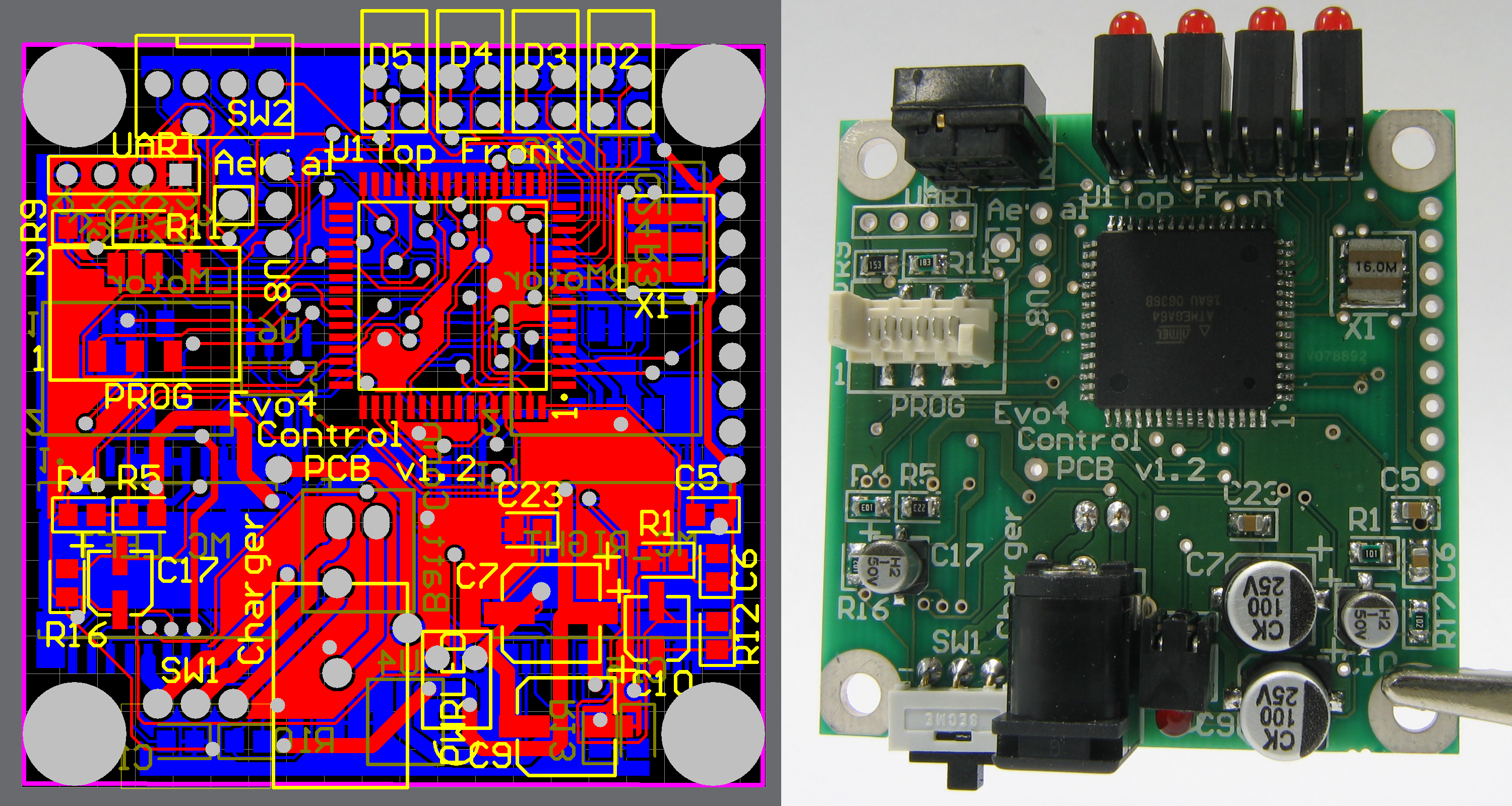
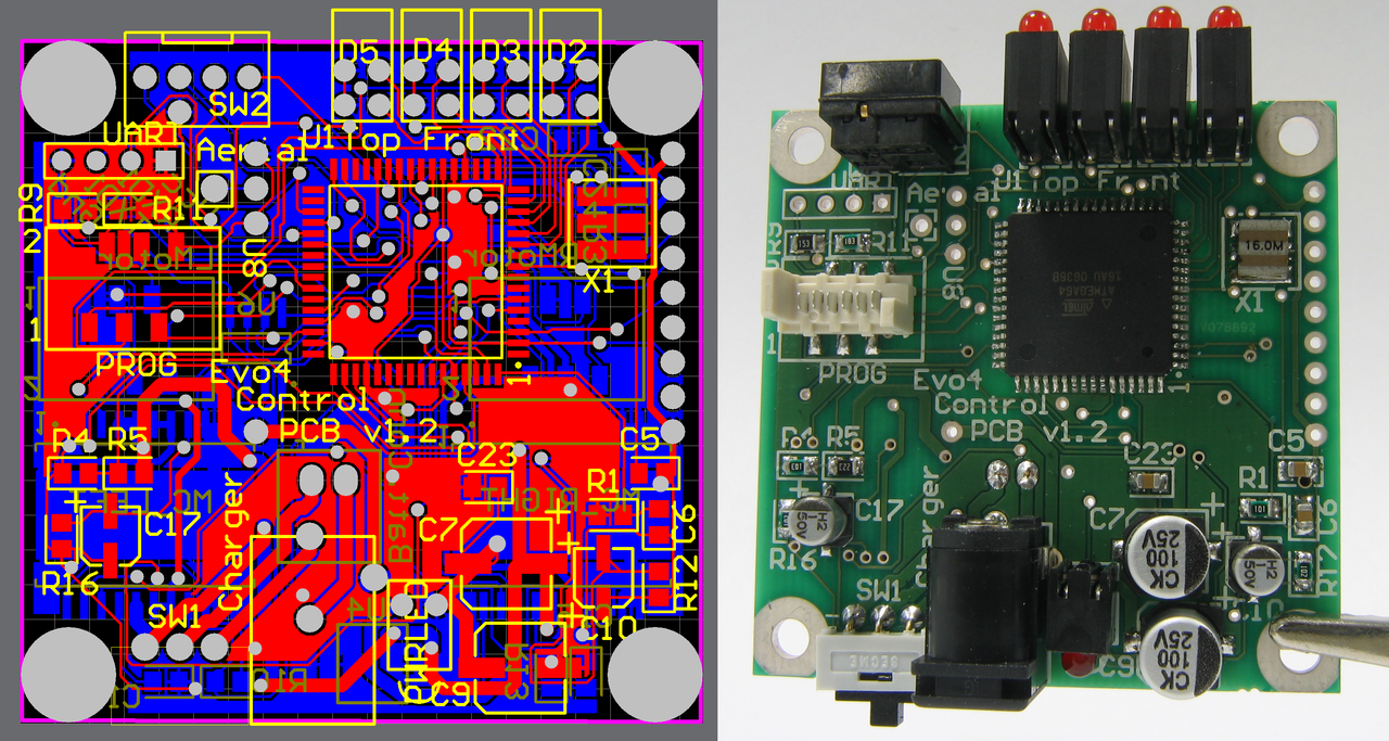
English: This picture shows (left) a printed circuit board (PCB) layout, created on a computer and (right) the manufactured board, populated with parts. Both through-hole and surface mounts components have been used; the board is double-sided, with through-hole plating, green solder resist, white solder paste (visible on unsoldered holes, such as the four corner mounting holes and the nine holes down the right hand side of the board) and white silkscreen printing.
Italiano: Progetto di un circuito stampato a sinistra e realizzazione a destra.
Deutsch: Links das im CAD erstellte Layout einer Leiterplatte, in dem die verschiedenen Lagen mit unterschiedlichen Farben dargestellt sind. Rechts die daraus hergestellte und mit Bauelementen bestückte Leiterplatte.
Español: A la izquierda la imagen de la PCB diseñada por ordenador y a la derecha la PCB manufacturada y montada.
Svenska: Datordesign av ett mönsterkort (vänster) och det färdiga kretskortet (höger)
中文:印刷電路板
Magyar: A baloldalon egy NYÁK CAD program segítségével tervezett rajza, a jobboldalon pedig a rajznak megelelően elkészített panel látható.
Bahasa Indonesia: Foto dari desain sirkuit dan realisasinya
한국어: 컴퓨터로 설계된 인쇄회로기판 (왼쪽) 및 기판과 부품이식된 실장 (오른쪽). 기판은 홀로 통하는 도금, 녹색 땝납 저항, 흰 땝납 페이스트, 흰 실크스크린 프린트가 있는, 양면이다. 양쪽 표면 실장과 홀로 통하는 부품은 사용되었다. |
||
| 日付 | |||
| 原典 | Photographed by User:Mike1024 | ||
| 作者 | User Mike1024 | ||
| 許可 (ファイルの再利用) |
|
ファイルの履歴
過去の版のファイルを表示するには、その版の日時をクリックしてください。
| 日付と時刻 | サムネイル | 寸法 | 利用者 | コメント | |
|---|---|---|---|---|---|
| 現在の版 | 2007年2月2日 (金) 19:10 | | 3,000 × 1,600 (2.74メガバイト) | Mike1024 | {{Information| |Description=This picture shows (left) a printed circuit board (PCB) layout, created on a computer and (right) the manufactured board, populated with parts. Both through-hole and surface mounts components have been used; the board is double |
ファイルの使用状況
以下のページがこのファイルを使用しています:
グローバルなファイル使用状況
以下に挙げる他のウィキがこの画像を使っています:
- ast.wikipedia.org での使用状況
- ca.wikipedia.org での使用状況
- de.wikipedia.org での使用状況
- en.wikipedia.org での使用状況
- es.wikipedia.org での使用状況
- et.wikipedia.org での使用状況
- eu.wikipedia.org での使用状況
- fr.wikipedia.org での使用状況
- fr.wiktionary.org での使用状況
- hi.wikipedia.org での使用状況
- hi.wikiversity.org での使用状況
- hu.wikipedia.org での使用状況
- id.wikipedia.org での使用状況
- it.wikipedia.org での使用状況
- ko.wikipedia.org での使用状況
- ne.wikipedia.org での使用状況
- pt.wikipedia.org での使用状況
- ru.wikipedia.org での使用状況
- sv.wikipedia.org での使用状況
- vi.wikipedia.org での使用状況
- zh.wikipedia.org での使用状況